Large area topography of silicon Wafer

Inquiry number
SOL-0000001221
Beamline
BL20B2 (Medical and Imaging I)
Scientific keywords
| A. Sample category | inorganic material |
|---|---|
| B. Sample category (detail) | semiconductor, solid-state crystal |
| C. Technique | X-ray diffraction |
| D. Technique (detail) | single crystal |
| E. Particular condition | 2D imaging |
| F. Photon energy | X-ray (4-40 keV) |
| G. Target information | dislocation, strain |
Industrial keywords
| level 1---Application area | Semiconductor |
|---|---|
| level 2---Target | silicon semiconductor |
| level 3---Target (detail) | SOI, substrate |
| level 4---Obtainable information | d-spacing (lattice parameter), crystal structure |
| level 5---Technique | diffraction, imaging |
Classification
A80.12 semiconductor, M10.80 stress strain
Body text
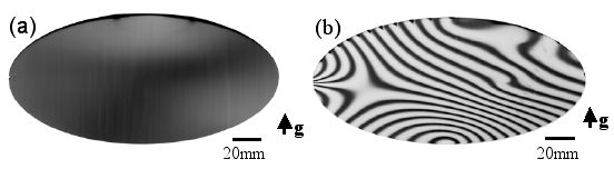
When a 200- or 300-mm diameter (001) Si wafer is irradiated with a monochromatic beam of 300-mm (H) x 2-mm (V) in size at a glazing angle of less than 0.38°, X-ray irradiation covers the whole area of the wafer. Under this condition, tuning the X-ray energy to 21.45 keV enables us to realize the Berg-Barrett X-ray topography using the asymmetric 115 reflection. Combination of this topographic technique and local-area rocking curve measurements reveals the crystal perfection of the wafer surface. Examples of the characterization of surface strain caused by each step of 200-mm diameter CZ-Si wafer fabrication processes are shown in figure. (a) 1-shot X-ray topograph of the whole area of a lapped surface which gave a broad rocking curve. (b) Step scanned X-ray topograph of a mechanically and chemically polished (MCP) surface. In this case, the wafer was rotated at a step interval of 10 arcsec and the exposure was repeated at each step to obtain so-called zebra patterns because the rocking curve was sharp and the wafer was warped. The warpage can be evaluated from the stripe patterns.
Source of the figure
Original paper/Journal article
Journal title
S. Kawado et al.: J. Synchrotron Rad. 9 (2002) 166-168, S. Kawado: Materials Science in Semiconductor Processing 5 (2003) 435-444
Figure No.
Technique
This topography experiment has been done using 300-mm wide beam at medium-length beamline 20B2
Source of the figure
No figure
Required time for experimental setup
1 shift(s)
Instruments
References
| Document name |
|---|
| S. Kawado: Materials Science in Semiconductor Processing 5 (2003) 435-444 |
| S. Kawado et al.: J. Synchrotron Rad. 9 (2002) 166-168 |
Related experimental techniques
Questionnaire
The measurement was possible only in SPring-8. Impossible or very difficult in other facilities.
This solution is an application of a main instrument of the beamline.
Ease of measurement
Middle
Ease of analysis
With a great skill
How many shifts were needed for taking whole data in the figure?
Less than one shift