Graphene Nanopatterning Techniques (Press Release)
- Release Date
- 14 Jun, 2013
- BL17SU (RIKEN Coherent Soft X-ray Spectroscopy)
Tohoku University
Japan Synchrotron Radiation Research Institute (JASRI)
|
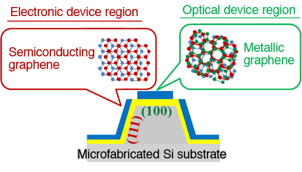
Hirokazu Fukidome (associate professor) of the Research Institute of Electrical Communication, Tohoku University (President, Susumu Satomi), in collaboration with the School of Engineering, Tohoku University, and JASRI (President, Tetsuhisa Shirakawa), succeeded in establishing a site-selective crystal growth technique for graphene*1 on a microfabricated Si substrate for the first time in the world. Their achievement will open the way to the development of devices based on the fusion of graphene and Si, which are promising next-generation materials. This technique will become the basic technology for manufacturing three-dimensional graphene-based multifunctional integrated circuits. The details of this research were published in the journal of the Institute of Electrical and Electronics Engineers (IEEE) Proceedings of the IEEE on 15 June 2013. Publication: |
<<Figures>>
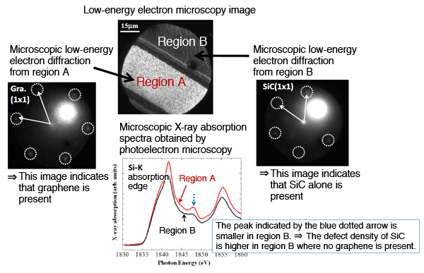
by low-energy electron microscopy*2 and photoelectron microscopy*3
The peak indicated by the blue dotted arrow is small when the defect density of SiC is high.
<<Glossary>>
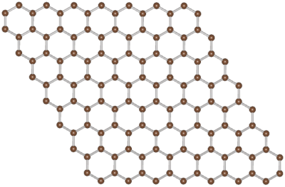
*1 Graphene
A monolayer of graphite crystals consisting of carbon atoms arranged in a honeycomb hexagonal network to form a two-dimensional sheet, as shown in the figure below. Graphene has both semiconducting and metallic properties and is expected to serve as a post-Si material. Carbon nanotubes are obtained by rolling graphene into cylindrical shapes.
*2 Low-energy electron microscopy
A microscopy method of irradiating the surface of samples with electron beams at low accelerating voltages ranging from 2-30 V and the backscattered electron beams are enlarged and projected using a lens. By low-energy electron microscopy, low-energy electron diffraction (microscopic electron diffraction) patterns from a nanoscale region can be obtained to reveal the details of surface atomic arrangement. Moreover, the digital measurement method for determining the number of graphene layers, developed by Dr. Hibino of NTT Basic Research Laboratories, has become the basic technology in research on graphene.
*3 Photoelectron microscopy
A spectroscopic method having spatial resolution realized by the combination of photoelectron spectroscopy, low-energy electron diffraction, and microscopy. The behavior of electrons on a solid surface can be visualized by this method with a resolution of 20-30 nm. This method is used in a wide range of applications, from nanoscale devices and planetary science.
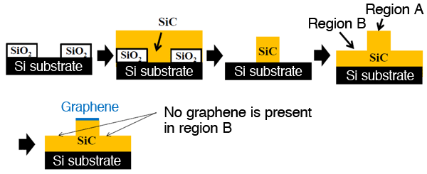
*4 Micro-electromechanical systems (MEMS)
MEMS are devices in which sensors, actuators, and electronic circuits are integrated on a single substrate (e.g., Si substrate).
|
For more information, please contact: Dr. Masato Kotsugi (JASRI) |


- Previous Article
- Clarification of Crystal Structure of Calcium Having Highest Superconducting Transition Temperature among All Elements (Topic)
- Current article
- Graphene Nanopatterning Techniques (Press Release)