Development of High-Performance X-ray Image Detector as “Eye” of SPring-8 Angstrom Compact Free-Electron Laser (SACLA) Facility (Press Release)
- Release Date
- 15 Mar, 2014
- SACLA
RIKEN
Japan Synchrotron Radiation Research Institute (JASRI)
Institute for Molecular Science, National Institute of Natural Sciences
Key Points
• Functioning as the “eye”of the SACLA facility to obtain data of objects irradiated with SACLA
• Successful development of the X-ray image detector, an essential technology used in SACLA
• One of the World’s highest total performance and greatest stability at X-ray Free-Electron Laser facility realized using the advanced technologies of charge-coupled device (CCD) sensors
|
RIKEN (Ryoji Noyori, President) and JASRI (Yoshiharu Doi, President) have succeeded in developing an X-ray image detector, the multi-port charge-coupled device (MPCCD) detector, that is optimized for experiments conducted using SACLA,*1 an X-ray free-electron laser (XFEL). An international collaborative research group led by Takaki Hatsui (team leader) of the Data Acquisition Team, Beam Line Research and Development Group, RIKEN SPring-8*3 Center (Tetsuya Ishikawa, Director); Takashi Kameshima (research scientist) of the XFEL Utilization Division, JASRI; Toshio Horigome (section chief) of the Optical Technology Section, Technical Division, Institute for Molecular Science; Hajime Murao (chief enginner) of Meisei Electric Co., Ltd.; David Burt (chief engineer) of e2V, UK; and Andrew Holland (chief technology officer) and Karen Holland (chief executive officer) of XCAM Ltd., UK. This research was partially supported by the X-ray Free-Electron Laser Priority Strategy Program, Ministry of Education, Culture, Sports, Science and Technology. The results of this study were published online in the American scientific journal Review of Scientific Instruments on 14 March 2014 Vol. 85, Article number 033110. Publication: |
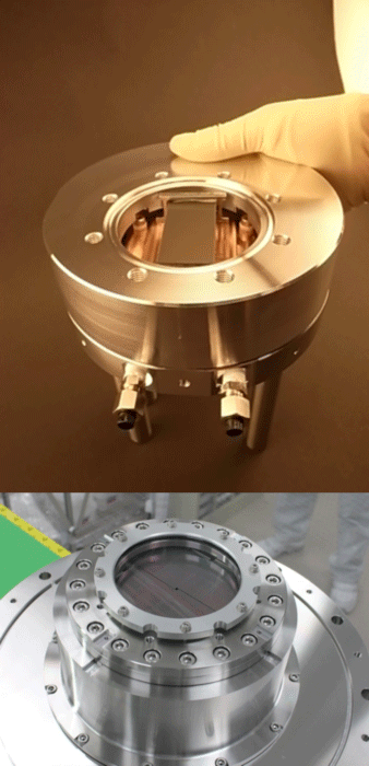
(Upper) Example of X-ray image detector with a CCD sensor. This is cooled to approximately -20℃ in vacuum for use in the experiment.
(Lower) Multiport detector with eight CCD sensors to realize a large-area image region. The sensors can be arranged with a gap between image area of 0.3 mm and can detect emitted X-rays without deteriorating the performance of sensors.
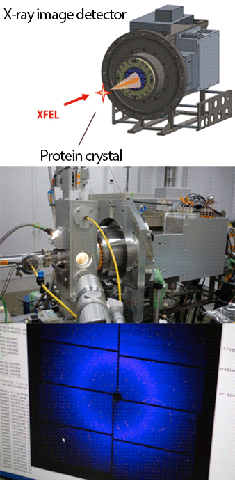
(Upper) Schematic of protein structure analysis experiment
(Middle) Equipment used in experiment
(Lower) Data of protein structure obtained in experiment (under analysis)
《Glossary》
*1 X-ray free-electron laser (XFEL), SACLA
SACLA is the most compact X-ray Free Electron Laser (XFEL) facility in the world, and is also now the only XFEL operating below 1 Å wavelength. SACLA was built jointly by RIKEN and JASRI as one of the Key Technologies of National Importance, and was completed in March 2011. SACLA's benefits include short wavelength and pulse-width, enabling the observation of living organisms and materials at the atomic level. Significantly, the close proximity between SACLA and the large synchrotron radiation facility SPring-8 enables collaborative projects using both XFEL and bright SR.
*2 Charge-coupled device (CCD) sensor
A CCD sensor consists of a conversion unit that converts X-rays and visible light into electric charges and a structural unit to transfer the generated electric charges. The latter unit has a metal-insulator-semiconductor (MIS) structure.*4
*3 SPring-8
A large synchrotron radiation facility that generates the highest-quality synchrotron radiation, located in Hyogo prefecture, Japan. Owned by Riken, and operated by JASRI. The nickname SPring-8 is short for Super Photon ring-8 GeV. Synchrotron radiation refers to the strong and highly oriented electron magnetic waves generated when the orbit of electrons, accelerated to a near-light speed, is bent by magnetic field. Applications of the synchrotron radiation produced by SPring-8 includes nanotechnology, biotechnology and industrial use.
*4 Metal-insulator-semiconductor (MIS) structure
The MIS structure consists of a semiconductor layer, an insulator layer, and a metal layer, from the bottom. In a CCD sensor, signal charges trapped in the semiconductor layer are moved by changing the voltage applied to the metal layer. Silicon oxide used as the insulator layer is charged by X-ray irradiation, disturbing the operation of the CCD sensor. By adopting a “radiation hard”structure that minimizes the charging effect, the research group succeeded in developing a detector applicable to XFEL experiments, which had been considered to be impossible with a conventional CCD process.
|
For more information, please contact: |
- Previous Article
- Electron dynamics in copper oxide superconductors unveiled by three inelastic-scattering techniques (Press Release)
- Current article
- Discovery of a New Crystal Structure Family of Oxide-Ion Conductors NdBaInO4 (Press Release)