Development of X-Ray Microscope Enabling Visualization of Electron Density Distribution of Materials with Nanometer Resolution (Press Release)
- Release Date
- 20 Apr, 2010
- BL29XU (RIKEN Coherent X-ray Optics)
- Observing Inside of Hollow Metallic Nanoparticles by X-Ray Computed Tomography (CT) with the World's Highest Resolution
Osaka University
Hokkaido University
Kyoto University
RIKEN
Key research findings
• Realization of X-ray computed tomography (CT) technology enabling three-dimensional observation of electron density distribution of materials
• Visualization of internal structure of 200-nm-breadth hollow metallic nanoparticles with spatial resolution higher than 10 nm
• Potential application of developed X-ray microscope to analysis of monomolecular structures using X-ray free-electron laser
|
Scientists at Osaka University (Kiyokazu Washida, President) have developed an ultimate X-ray microscope that enables the three-dimensional observation of the electron density distribution of materials with a spatial resolution higher than 10 nm (a nanometer is one-billionth of a meter) for the first time in the world. They succeeded in observing the detailed internal structure of hollow Au/Ag nanoparticles (Au/Ag nanoboxes) with a breadth of about 200 nm that were synthesized by shape control. This was achieved by the following scientists: Graduate School of Engineering (Akio Baba, Chairman), Osaka University: Yukio Takahashi, a specially appointed researcher, Nobuyuki Zettsu, an assistant professor, Ryosuke Tsutsumi, a graduate student, and Kazuto Yamauchi, a professor; Hokkaido University (Hiroshi Saeki, President): Yoshinori Nishino, a professor and former senior research scientist at Ishikawa's Coherent X-Ray Optics Laboratory at RIKEN; Kyoto University (Hiroshi Matsumoto, President): Eiichiro Matsubara, a professor; RIKEN (Ryoji Noyori, President): Tetsuya Ishikawa, the director and chief scientist at RIKEN SPring-8 Center. When observing the nanostructure of a material three-dimensionally, electron beam tomography*1 with a transmission electron microscope is generally used; however, such an observation is difficult for metals with a thickness of 100 nm or more because electron beams are not sufficiently transmitted through such thick metals. In this study, the research group developed a novel X-ray microscope using highly coherent high-density X-rays obtained through Kirkpatrick-Baez (KB) mirrors at SPring-8. The group succeeded in quantitatively visualizing the electron density distribution of a 200-nm-thick Au/Ag nanobox. The spatial resolution of the developed X-ray microscope, which is higher than 10 nm, is thought to be the highest X-ray CT*2 resolution in the world. The result of this research indicated that the quantitative structural analysis of nanostructured materials, such as metallic nanoparticles, nanowires, and quantum dots, is possible using the developed X-ray microscope and is expected to lead to greater understanding of the mechanisms by which properties specific to nanostructures are manifested and to the design and development of innovative nanomaterials. When this X-ray microscope is combined with an X-ray free-electron laser,*3 which is being developed and the facilities of which are being constructed by RIKEN, the resolution and speed are expected to further increase, thus paving the way for its application to important medical research, for example, the monomolecular structural analysis of membrane proteins, a key to developing new drugs. This research was supported by the "Promotion of Improvement of Independent Research Environment for Young Scientists" program*4 under the Special Coordination Fund for Promoting Science and Technology. It was also supported by a research project for promoting the use of X-ray free-electron lasers by the Ministry of Education, Culture, Sports, Science and Technology (MEXT) and by Grants-in-Aid for Scientific Research from the Japan Society for the Promotion of Science and MEXT. The achievements of this research were published in the online version of the scientific journal Nano Letters on 19 April 2010, prior to the printed version on 12 May 2010. Publication: |
<Figure>
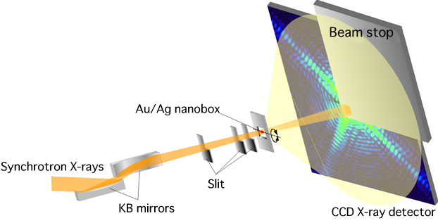
Synchrotron X-rays are focused on a 1-μm-diameter spot through KB mirrors, and a sample (Au/Ag nanobox) is placed on the spot. The intensity distribution of X-rays elastically scattered in the forward direction (coherent X-ray diffraction patterns) is measured by a charge-coupled device (CCD) X-ray detector. The obtained coherent X-ray diffraction patterns are processed by a computer to reconstruct a three-dimensional image of the sample structure. In the reconstruction, coherent X-ray diffraction patterns from different incident angles, obtained by rotating the sample, are used.
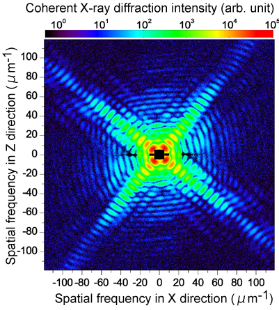
The coherent X-ray diffraction patterns of a Au/Ag nanobox were successfully observed with a high contrast. These patterns are composed of spots. Each spot is generated by the interference enhancement of elastically scattered X-rays, and the patterns indicate the fine structure of nanoparticles.
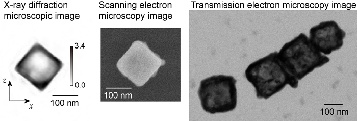
By X-ray diffraction microscopy, the hollow structure inside a Au/Ag nanobox is clearly observed and the electron density distribution is quantitatively visualized. However, the scanning electron microscopy image only provides information on the surface of the Au/Ag nanobox and cannot show its internal structure. In the transmission electron microscopy image, hollow structures can be observed, but they are blurred because of the insufficient transmission of electrons, and the quantitative analysis of the image is difficult because of the multiple scattering of electrons.
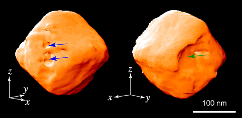
A three-dimensional electron density distribution is obtained by performing a phase retrieval calculation with respect to the coherent X-ray diffraction patterns of a Au/Ag nanobox observed with different X-ray incident angles. The detailed surface structure of the Au/Ag nanobox can be observed when an equivalent-electron-density plane is displayed. Small pits and a large pit are confirmed at the positions indicated by the blue and green arrows, respectively.
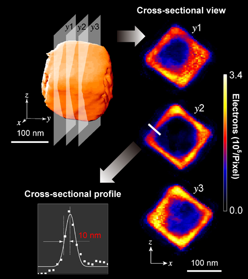
Cross-sectional views of a Au/Ag nanobox can be obtained by slicing the image of its three-dimensional electron density distribution at arbitrary cross sections. In addition, the obtained cross-sectional images can be displayed as two-dimensional electron density distributions. The spatial resolution of the cross-sectional profiles was found to be higher than 10 nm by analyzing the cross section of the thinnest structure in the cross-sectional images.
<Glossary>
*1 Tomography
Tomography is one of the inverse analysis technologies used for geophysical exploration, medical diagnosis, and other applications. In most tomographic technologies, the distributions of various internal properties of a material are visualized by arranging scan lines to surround a target region.
*2 X-ray computed tomography (CT)
X-ray CT is a method of reconstructing the three-dimensional image of a sample from its radiographs obtained from different angles. X-ray CT is widely used in clinical examinations at hospitals and nondestructive tests in industry.
*3 X-ray free-electron laser
An X-ray free-electron laser is a next-generation technology that produces X-rays with perfect coherency. X-ray free-electron laser facilities are being developed in Japan, the US, and European countries. In Japan, RIKEN is constructing an X-ray free-electron laser in the campus of SPring-8 in cooperation with Japan Synchrotron Radiation Research Institute. The X-ray free-electron laser has been designated as a national critical technology.
*4 "Promotion of Improvement of Independent Research Environment for Young Scientists" program
With the aim of fostering research scientists who can play active roles worldwide, research organizations that are systematically working to improve their research environment and encourage the independence of young scientists are attempting to create a more dynamic research environment by promoting the introduction of a tenure-track system. In the tenure-track system, young scientists accumulate experience in research and teaching in independent research environments under fixed-term (tenured) employment and are provided with a career path leading to their employment as faculty staff members upon passing the final review.
For more information, please contact: |

- Current article
- Development of X-Ray Microscope Enabling Visualization of Electron Density Distribution of Materials with Nanometer Resolution (Press Release)