Clarifying the Mechanism of Transparent Cobalt-Doped Titanium Dioxide Thin Films Exhibiting Magnetism (Press Release)
- Release Date
- 24 Jan, 2011
- BL17SU (RIKEN Coherent Soft X-ray Spectroscopy)
- BL29XU (RIKEN Coherent X-ray Optics)
RIKEN
Japan Synchrotron Radiation Research Institute
Key research findings
○ Discovery that titanium (Ti) 3d electrons control the spins of cobalt (Co) 3d electrons sparsely distributed in thin films
○ Clarifying that thin films have a semiconductor surface and a metallic bulk
○ Providing guidelines for the design of materials and devices for spintronics
|
Scientists from RIKEN (President, Ryoji Noyori) and Japan Synchrotron Radiation Research Institute (JASRI; President, Tetsuhisa Shirakawa) have clarified, for the first time in the world, that cobalt-doped titanium dioxide (Co:TiO2) thin films, a promising candidate for spintronics*1 materials, exhibit ferromagnetism when Ti 3d electrons*2 freely move and align the spins of Co 3d electrons sparsely distributed in the films. This achievement was obtained by a joint research group led by Shik Shin (Leader of the Excitation Order Research Team, Quantum Order Research Group, RIKEN SPring-8 Center (Director, Tetsuya Ishikawa), who is also a professor at the Institute for Solid State Physics, The University of Tokyo), Takumi Ohtsuki (Research Scientist of Professor Shin’s group), and Haruhiko Ohashi (Associate Chief Scientist) and Yasunori Senba (Research Scientist) of JASRI. Our daily lives are supported by electronics technologies that separately use two properties of electrons, i.e., electric conductivity and magnetism. Recently, spintronics, which uses these properties simultaneously, has been attracting attention as a means of developing new materials and functions. The research group analyzed in detail the electron state of Co:TiO2 thin films, a promising candidate for spintronics materials, obtained by doping a small amount of Co atoms into titanium dioxide (TiO2), by X-ray photoelectron spectroscopy*3 at SPring-8. Through this analysis, they clarified that the ferromagnetism of Co:TiO2 thin films is mediated by Ti 3d electrons that freely move around the thin films and align the spins of Co 3d electrons sparsely distributed in the film. In addition, they analyzed Co:TiO2 thin films by making full use of photoelectron spectroscopy with hard X-rays (wavelength, approximately 0.16 nm) and soft X-rays (wavelength, approximately 1 nm). From the analytical results, it was clarified that the surface of the Co:TiO2 thin films exhibits semiconducting properties because of the absence of the Fermi edge,*4 which gives a material metallic properties, whereas the bulk exhibits metallic properties because of the presence of the Fermi edge. Thus, they found a difference in electric conductivity between the surface and the bulk of Co:TiO2 thin films. These results indicate the suitability of Co:TiO2 thin films as a material for spintronics and provide guidelines for their practical application. The results of this research were published online in the American scientific journal Physical Review Letters on 28 January 2011 prior to the publication of the printed version. (Publication) |
<<Glossary>>
*1 Spintronics
In spintronics, it is attempted to simultaneously use the electric charges and spins of electrons that constitute materials. Spintronics was coined from "spin" and "electronics." The aim of spintronics is to realize new functions that cannot be achieved with conventional technologies that use electric charges and spins separately. Currently used spintronics devices include reading heads for hard discs.
*2 3d electrons
3d electrons refer to the electrons in the 3d orbital (an electron orbital of atoms). For transition metals with atomic numbers from 21 to 30, the 3d orbital is the outermost orbital, and the arrangement of electrons in the 3d orbital determines the properties of individual materials.
*3 X-ray photoelectron spectroscopy
X-ray photoelectron spectroscopy is a method of examining the electron state of materials by irradiating X-rays onto a material and determining the relationship between the number and energy of electrons expelled from the surface of the material. This method enables direct observation of the energy distribution of electrons in materials. Both hard and soft X-rays as well as other types of light are used in X-ray photoelectron spectroscopy.
*4 Fermi edge
In crystals, electrons occupy energy bands generated by the periodicity of crystals, starting from the band with lowest energy. In the case of metals, electrons occupy lower-energy bands, generating a boundary between the energy bands filled with electrons and empty energy bands. The energy level of this boundary is called the Fermi level. When the electron energy of metals near the Fermi level is measured by photoelectron spectroscopy, it is observed that the spectral intensity discontinuously increases from 0 at the Fermi level. This is called the Fermi edge.
<<Figure>>
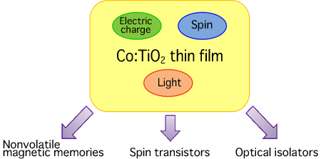
their application as spintronics materials
Co:TiO2 thin films combine electric conductivity and magnetism, and are highly expected to be used as a material for spintronics, a research field aimed at the simultaneous use of these properties. In addition, Co:TiO2 thin films can be used as transparent magnets because they are almost transparent to visible light. The practical realization of spintronics devices, such as nonvolatile magnetic memories, spin transistors, and optical isolators, will lead to major advances in the conventional electronics industry.
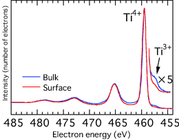
Trivalent Ti ions with an electron in the 3d orbital, i.e., Ti3+ (shown by the arrow), are more widespread in the bulk of a thin film than on its surface.
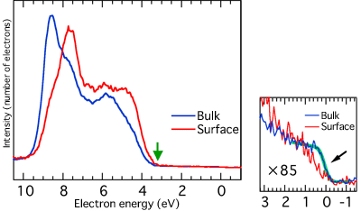
For TiO2 without Co doping, no peak intensity is observed at electron energies to the right of the green arrow (0 – 3.5 eV) because this energy region corresponds to a band gap where no electrons exist. When the region near the electron energy of 0 is magnified, however, unknown components are observed in the band gap of the Co:TiO2 thin film (right figure). The bulk of the thin film (blue line) exhibits metallic properties because of the presence of the Fermi edge (black arrow), whereas the surface of the thin film (red line) exhibits semiconducting properties because of the absence of the Fermi edge.
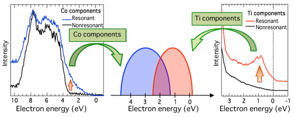
The 3d components of Co and Ti atoms are enhanced (orange arrows) in the left and right figures, respectively. As a result, the Co 3d components responsible for the magnetism overlap with the Ti 3d components responsible for the electric conductivity (central figure). This overlapping indicates the interaction between the Co and Ti 3d electrons; the spins of the Co 3d electrons sparsely distributed in the thin films are aligned by the Ti 3d electrons.
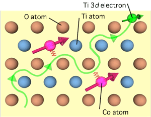
When Co atoms are doped into TiO2, which comprises Ti and O atoms, Ti atoms are replaced by Co atoms. Ti 3d electrons freely move around TiO2 and act on the Co 3d electrons to align their spins in the direction indicated by red arrows, causing the thin film to exhibit ferromagnetism.
|
For more information, please contact: |


- Current article
- Clarifying the Mechanism of Transparent Cobalt-Doped Titanium Dioxide Thin Films Exhibiting Magnetism (Press Release)