Paving the Way for Development of Multifunctional Devices Consisting of Graphene on a Silicon Substrate (Press Release)
- Release Date
- 08 Nov, 2011
- BL17SU (RIKEN Coherent Soft X-ray Spectroscopy)
- BL23SU (JAEA Actinide Science)
Research Institute of Electrical Communication, Tohoku University
Hirokazu Fukidome (Assistant Professor) and his colleagues at the Research Institute of Electrical Communication (RIEC), Tohoku University, have succeeded in developing a next-generation multifunctional electronic material, graphene on silicon (GOS), by the separation of metallic and semiconducting properties using the crystallographic orientation of the silicon (Si) substrate. They have also demonstrated that the integration of transistors using GOS is possible. The feasibility of multifunctional graphene integrated circuits using currently available semiconductor integration technology has been demonstrated, and this breakthrough achievement paves the way for multifunctional graphene integrated circuits. Hirokazu Fukidome, Maki Suemitsu (Professor), and Taiichi Otsuji (Professor) of RIEC, Tohoku University (President, Akihisa Inoue), carried out this research under the title "Development of Graphene-on-Silicon Material/Device Technologies," with Taiichi Otsuji as the team leader, as part of the research project "Research of Innovative Materials and Processes for Creation of Next-Generation Electronics Devices" (Research Supervisor: Hisatsune Watanabe, also CEO of Selete), supported by Core Research for Evolutional Science and Technology (CREST) of Japan Science and Technology Agency (President, Michiharu Nakamura). They collaborated with Yuden Teraoka (Principal Researcher) and Akitaka Yoshigoe (Assistant Principal Researcher) of the Quantum Beam Science Directorate of Japan Atomic Energy Agency (JAEA; President, Atsuyuki Suzuki); and Toyohiko Kinoshita (Chief Scientist), Masato Kotsugi (Research Scientist), and Takuo Ohkouchi (Research Scientist) of the Research and Utilization Division of the Japan Synchrotron Radiation Research Institute (JASRI; President, Tetsuhisa Shirakawa). The research group succeeded in developing a next-generation multifunctional electronic material, graphene*1 on silicon (GOS), by the separation of metallic and semiconducting properties using the crystallographic orientation of the Si substrate. They also demonstrated that the integration of field-effect transistors*2 using GOS is possible. The feasibility of multifunctional graphene integrated circuits using currently available semiconductor integration technology has been demonstrated, and this breakthrough achievement paves the way for multifunctional graphene integrated circuits. A two-dimensional layer of carbon atoms, known as a graphene, has carrier mobility*3 that is a hundredfold that of Si and is thermally and chemically stable. Therefore, the development of graphene as a next-generation device material has been competitively pursued worldwide. RIEC has already developed technologies related to GOS. Using such technologies, a graphene layer can be grown on the surface of a single-crystal SiC layer formed on a Si substrate. Professor Suemitsu and his colleagues fabricated GOS for the first time in the world, and Professor Otsuji and his colleagues developed prototype field-effect transistors using GOS. Because the mature fabrication technology of silicon devices can be used for the fabrication of GOS without alteration, GOS has been attracting attention as a promising material that can help realize practical applications of graphene. The high carrier mobility of graphene alone is not sufficient to allow graphene to replace the materials used in conventional silicon devices. Therefore, the research group has been attempting to develop a technology that is unique to GOS. In this study, it was found that surface and interfacial structures and the band structure of graphene can be controlled by changing the crystallographic orientation of the Si substrate. Although it is known that the band structure of graphene can be controlled by changing the crystallographic orientation of an expensive SiC crystal substrate, this is the first time that the feasibility of similar control has been demonstrated on an inexpensive large-area Si substrate. This achievement is expected to enable the production of graphene that is suitable for various device applications. The achievement of this study was published online in Applied Physics Express, published by the Japan Society of Applied Physics, on 9 November 2011 under the title "Control over structural and electronic properties of epitaxial graphene by tuning surface termination of 3C-SiC(111)/Si" and in Journal of Materials Chemistry, published by the Royal Society of Chemistry, under the title "Control of Epitaxy of Graphene by Crystallographic Orientation of a Si Substrate toward Device Applications." Publication: "Control of epitaxy of graphene by crystallographic orientation of a Si substrate toward device applications" |
<<Glossary>>
*1 Graphene
Graphene is a monolayer of graphite crystals. Carbon atoms form a two-dimensional sheet with a honeycomb hexagonal network (Fig. 1). It has the properties of both semiconductors and metals and is expected to be used as a post-Si material. Carbon nanotubes can be obtained by forming cylinders of graphene.
*2 Field-effect transistor
A field-effect transistor is a transistor in which the current between the source and drain is controlled by applying a voltage to the gate electrode. It is used as a basic element in digital logic circuits, in which a gate controls the flow of electrons or holes utilizing the applied electric field to the channel immediately below the gate electrode.
*3 Carrier mobility
Carrier mobility characterizes the ease of electron transfer in a material. It is also called electron mobility. The improvement of carrier mobility is indispensable for realizing high-speed semiconductor devices.
<<Figures>>
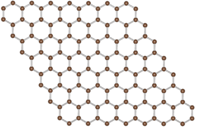
Two-dimensional honeycomb network of carbon atoms (spheres) on a plane. A monolayer of carbon atoms is called graphene, multiple layers of which form graphite.
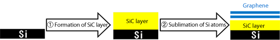
(1) A single-crystal SiC layer is grown on a single-crystal Si substrate by chemical vapor deposition.
(2) The obtained sample is heated at a high temperature in vacuum to form a graphene layer through the sublimation of Si atoms on the surface.
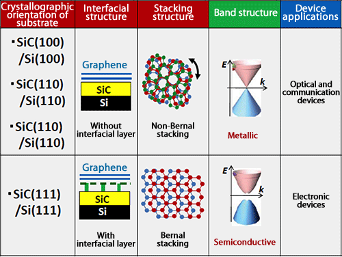
crystallographic orientations of Si substrate
SiC(111) is obtained when SiC is grown on Si(111). The crystallographic orientations of SiC and the Si substrate are the same. When a graphene layer is grown on a SiC(111)/Si(111) surface by heat treatment in vacuum, an interfacial layer is formed between the graphene and SiC layers. However, no interfacial layer exists in the case of other crystallographic orientations. When an interfacial layer exists, Bernal stacking occurs, i.e., several graphene layers slightly misaligned with each other; as a result, the obtained structure has semiconductive properties and is suitable for the fabrication of electronic devices. In contrast, without an interfacial layer, non-Bernal stacking occurs and the obtained structure has metallic properties and is suitable for the fabrication of optical and communication devices.
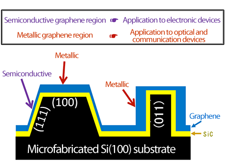
by three-dimensional microfabrication on Si substrate
In general, Si(100) substrates used for electronic devices have a (100) surface plane; planes perpendicular and oblique to the (100) substrate are the (011) and (111) planes, respectively. When SiC and then graphene layers are grown on these planes, the graphene layers grown on the (100) and (011) planes have metallic properties. In contrast, a graphene layer grown on the (111) plane has semiconducting properties, which enables the integration of circuits for both electronic and optical and communication devices on a single Si substrate.
|
For more information, please contact: |

- Previous Article
- Clarifying the Mechanism behind the Induction of Ferromagnetism in the Partial Absence of a Rare-Earth Element (Press Release)
- Current article
- Paving the Way for Development of Multifunctional Devices Consisting of Graphene on a Silicon Substrate (Press Release)