Successful Development of a Precision Graphene Production Control Method (Press Release)
- Release Date
- 06 Aug, 2012
- BL17SU (RIKEN Coherent Soft X-ray Spectroscopy)
Research Institute of Electrical Communication, Tohoku University
Japan Synchrotron Radiation Research Institute
|
The researchers (associate professor Hirokazu Fukidome, et al.) at Research Institute of Electrical Communication at Tohoku University, in collaboration with those at School of Engineering of Tohoku University, the University of Erlangen (Germany), Japan Synchrotron Radiation Research Institute, and Hirosaki University, successfully applied a microfabrication technique to the manufacturing of device structures, characterized by well-controlled (suppressed) nanoscale surface steps, on SiC substrates. The achievement translates into the development of a precision method for graphene*2 growth microscopically controlled in terms of electron state and the distribution of the numbers of stacked layers. Preparation of such substrates has been a challenge to be overcome for device applications of the next-generation electronic material: graphene. The results represent the realization of a technique to manipulate nanoscale electronic properties through the control of the number of graphene layers, which has a huge implication for accelerated commercialization of reliable next-generation electronic/optical devices, i.e. graphene-based devices. The details of the research were reported in a paper published in Applied Physics Letters (American Institute of Physics, August 6). |
<<Figures>>
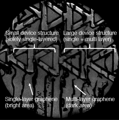
The diameter of the visual field corresponds to 50 micrometers. In large device structures and external areas, shades of black and white contrast are observed, indicating the existence of stacked graphene layers with different thicknesses. In small device structures, on the other hand, no contrast is observed, indicating an array of uniform monolayer graphenes.
its electron state as realized through microfabrication.
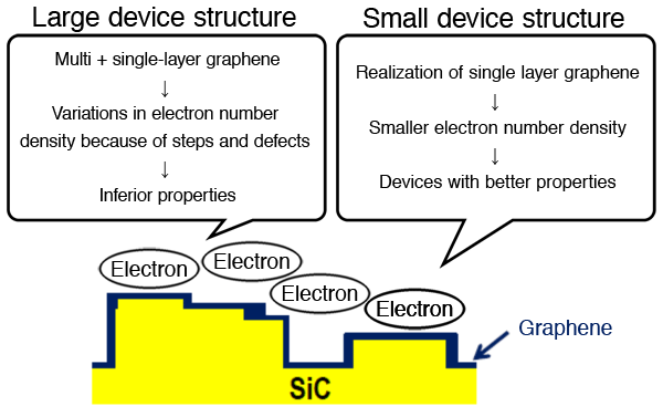
The large device structure has atomic steps on its surface, enabling a larger amount of electron doping. The smaller device structure has no atomic steps, forming uniform graphene with a smaller amount of electron doping. As this research indicates, controlling the device size provides possibilities to create an array of elements with different electric properties.
<<Glossary>>
*1 MEMS
MEMS (Microelectromechanical system) refers to the group of devices with a set of functionalities - sensors, actuators, and electronic circuitry - integrated on a substrate (e.g. silicon)
*2 Graphene
A one-atom thick sheet of graphite crystal. Carbon atoms are arranged in regular hexagonal networks (honeycomb structure), forming a two-dimensional sheet (Fig.3). Graphene is gathering high expectations as an effective post-silicon material owing to its unique combination of semiconductor and metallic properties. Carbon nanotubes are available by winding graphene into a tube.
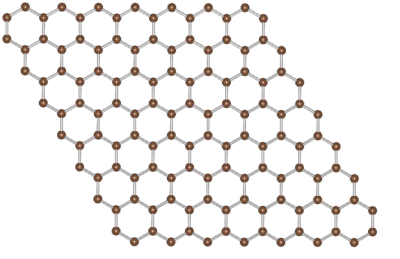
A graphene structure. Carbon atoms (balls) form a honeycomb network.
|
For more information, please contact: |

- Current article
- Successful Development of a Precision Graphene Production Control Method (Press Release)