Tracking charge carriers in the molecular crystal at organic pn junction
- Release Date
- 25 Mar, 2019
- BL19B2 (Engineering Science Research I)
In conventional organic solar cells, the electrons exhibit their particle-nature and need to jump between organic molecules in the cell. The conductivity is, therefore, lower than that of crystalline silicon solar cells. Researchers have succeeded to arrange the organic molecules in highly ordered manner like in crystals and to invoke the wave-nature. “Conductive bands” are formed by energy dispersive states and contribute to the high-carrier conductivity. It may improve the total efficiency of the cell.
An organic solar cell is light, flexible, low cost and green device, hence regarded as a potential seed of innovation in renewable energy industry. The efficiency of energy conversion of the organic solar cell is, however, lower than those of contemporary silicon solar cells.
In semiconductor solar cells, the light is converted into an energized pair of an electron (negative carrier) and a hole (positive carrier) at the “pn junction” interface at two semiconductor layers in the cell. Donor (electron pitching; p-type) and acceptor (electron catching; n-type) molecules in each layer of the semiconductors face each other as the ideal p/n junction. To increase the number of such solar “batteries” in the cell, the large area of pn junction is required, so that a complicated “bulkhetero” pn junction, which is a folded interface like pleats, has been developed. In such a complicated structure like a maze, the generated carriers are difficult to reach output electrodes of the cell, because the molecules are arranged roughly, in other words crystallinity is low (Fig. 1(a)). To realize a high transport efficiently, the carrier, an electron or a hole, should delocalize between molecules as a matter wave (Fig. 1(b)). The ordered arrangement of molecules brings out the wave-nature of the carries.
Researchers at Institute for Molecular Science (IMS), Japan Synchrotron Radiation Research Institute (JASRI) and Tokyo University of Science have succeeded to fabricate the organic semiconductor pn junction with high crystallinity. In the fabrication process of the junction, the acceptor (perfluoropentacene) molecules were deposited in well-ordered manner on to the single crystal of the donor molecules (pentacene) by the molecular beam epitaxy (MBE) technique. The electronic structures of the crystalline pn junction were observed by the angle-resolved photoelectron spectroscopy and showed the layer of the acceptor molecules form the valence band which is an evidence of invoking the wave-nature. The result of the present study shows that the MBE allows to fabricate the crystalline pn junction which may bring out the wave nature of both the electrons and the holes.
The functions of organic semiconductors can be tuned by designing the structures of constituent organic molecules. The fabrication technology of the crystalline pn junctions using a variety of organic molecules enables us to realize the new concept organic solar cells with high energy conversion efficiency.
Information of the paper:
Authors: Yasuo Nakayama, Ryohei Tsuruta, Naoki Moriya, Masataka Hikasa, Matthias Meissner, Takuma Yamaguchi, Yuta Mizuno, Toshiyasu Suzuki, Tomoyuki Koganezawa, Takuya Hosokai, Takahiro Ueba, Satoshi Kera
Journal Name: The Journal of Physical Chemistry Letters
Journal Title: “Widely Dispersed Intermolecular Valence Bands of Epitaxially Grown Perfluoropentacene on Pentacene Single Crystals”
DOI: 10.1021/acs.jpclett.8b03866
Financial Supports:
Organications:
Grant-in-Aid for Scientific Research, The Futaba Foundation, The Murata Science Foundation, The Precise Measurement Technology Promotion Foundation, Iketani Science and Technology Foundation
Numbers:
15H05498, 16K14102, 18H03904
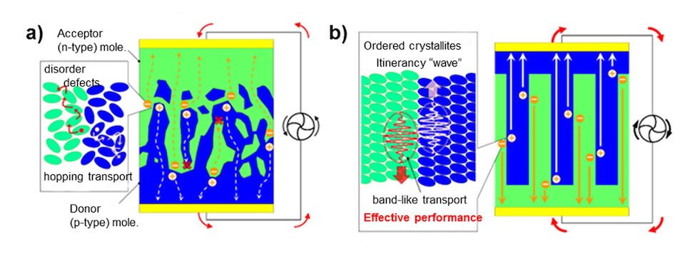
Crystal pn junction
(a) Hopping conduction in disordered junction, (b) band conduction in crystalline junction.
Contact Person: |
 ims.ac.jp
- Previous Article
- Successful tracking of single biomolecule motion with extremely low-dose X-ray (Press Release)
- Current article
- Tracking charge carriers in the molecular crystal at organic pn junction
- Next Article
- Pressure Makes Best Cooling(Press Release)