Structure-property relationship in a C60 FET thin film
問い合わせ番号
SOL-0000000964
ビームライン
BL02B2(粉末結晶構造解析)
学術利用キーワード
| A. 試料 | 有機材料 |
|---|---|
| B. 試料詳細 | 半導体, 結晶性固体, 低分子有機材料, 結晶, 膜 |
| C. 手法 | X線回折 |
| D. 手法の詳細 | 粉末結晶構造解析 |
| E. 付加的測定条件 | 表面, 室温 |
| F. エネルギー領域 | X線(4~40 keV) |
| G. 目的・欲しい情報 | 構造解析, 結晶構造, 機能構造相関 |
産業利用キーワード
| 階層1 | 半導体, ディスプレイ |
|---|---|
| 階層2 | LCD |
| 階層3 | TFT |
| 階層4 | 配向, 結晶化度 |
| 階層5 | 回折 |
分類
A80.12 半導体・電子材料, M10.20 粉末結晶回折
利用事例本文
Powder diffraction is a powerful technique to study crystal structures. Using this technique, one can measure structural parameters such as lattice parameters, atomic positions, etc of crystalline materials. By using synchrotron radiation one can also obtain charge density level structure closely related with physical properties as well as structural parameters. The figure shows diffraction data of a C60 FET thin film by low-glancing-angle X-ray diffraction. These data reveal a relationship between the structure and properties from the preferred orientation and crystallinity.
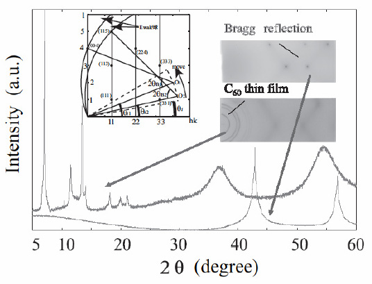
Fig. Low-glancing-angle X-ray patterns of a C60 FET thin film.
[ H. Ohashi, K. Tanigaki, S. Kimura, R. Kumashiro, K. Kato and M. Takata, Applied Physics Letters 84, 520-522 (2004), Fig. 1,
©2004 American Institute of Physics ]
画像ファイルの出典
BL評価レポート
ページ
61
測定手法
Powder diffraction using synchrotron radiations is a powerful technique to study crystal structures. The technique is applicable to thin films by low-glancing-angle X-ray diffraction and provides knowledge about the preferred orientation and crystallinity for thin films.
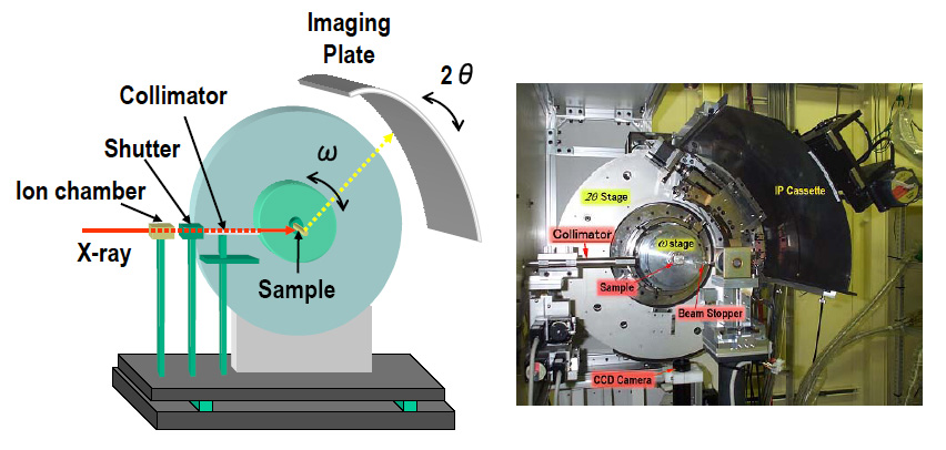
Fig. A large Debye-Scherrer camera.
画像ファイルの出典
BL評価プレゼン資料
測定準備に必要なおおよその時間
1 シフト
測定装置
| 装置名 | 目的 | 性能 |
|---|---|---|
| Large Debye-Scherrer camera | Powder diffraction | Camera radius: 286.48mm, Temperature: 15-1000K |
参考文献
| 文献名 |
|---|
| H. Ohashi et al., Applied Physics Letters, 84 (2004) 520. |
関連する手法
Single crystal structure analysis
アンケート
本ビームラインの主力装置を使っている
測定の難易度
中程度
データ解析の難易度
中程度
図に示した全てのデータを取るのにかかったシフト数
2~3シフト