High energy x-ray topography of silicon crystal ingots


Inquiry number
SOL-0000001109
Beamline
BL20B2 (Medical and Imaging I)
Scientific keywords
| A. Sample category | inorganic material |
|---|---|
| B. Sample category (detail) | semiconductor, solid-state crystal, crystal |
| C. Technique | X-ray diffraction |
| D. Technique (detail) | reflection, refraction |
| E. Particular condition | interface, room temperature |
| F. Photon energy | X-ray (4-40 keV), X-ray (> 40 keV) |
| G. Target information | dislocation, strain |
Industrial keywords
| level 1---Application area | Semiconductor |
|---|---|
| level 2---Target | silicon semiconductor |
| level 3---Target (detail) | SOI, substrate |
| level 4---Obtainable information | surface,interface, d-spacing (lattice parameter), crack, crevice, molphology |
| level 5---Technique | diffraction |
Classification
A80.10 electronics, A80.30 inorganic material, M10.80 stress strain
Body text
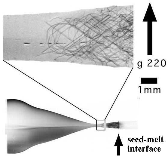
High energy (short wave length) x-ray topography is a powerful technique to visualize imperfection or inhomogeneity in a bulk crystal or a crystal containing heavy elements in a transmission geometry. Using this technique, one can observe lattice defects in a crystal ingot without any sample preparations such as cutting and slicing. The figure shows the 220 reflection traverse topograph of a 2 inches-diameter as-grown CZ-silicon crystal ingot. This topograph reveals the dislocation formation at the seed-melt interface and the dislocation termination during the necking process.
[ Y. Shikaura, S. Iida, S. Kawado, K. Mizuno, S. Kimura, J. Matsui, M. Umeto, T. Ozaki, T. Shimura, Y. Suzuki, K. Izumi, K. Kawasaki, K. Kajiwara and T. Ishikawa, Journal of Physics D 34, A158-A162 (2001), Fig. 6,
©2001 Institute of Physics and IOP Publishing, Ltd. ]
Source of the figure
Original paper/Journal article
Journal title
Y. Chikaura, S. Iida et al, J. Phys. D: Appl. Phys. 34 (2001) A158-A162.
Figure No.
Technique
Source of the figure
No figure
Required time for experimental setup
2 shift(s)
Instruments
References
| Document name |
|---|
| Y. Chikaura, S. Iida et al, J. Phys. D: Appl. Phys. 34 (2001) A158-A162. |
Related experimental techniques
Questionnaire
The measurement was possible only in SPring-8. Impossible or very difficult in other facilities.
This solution is an application of a main instrument of the beamline.
Ease of measurement
Middle
Ease of analysis
Easy
How many shifts were needed for taking whole data in the figure?
Two-three shifts