Plane-wave x-ray topography of grown-in microdefects in silicon crystals


Inquiry number
SOL-0000001144
Beamline
BL20B2 (Medical and Imaging I)
Scientific keywords
| A. Sample category | inorganic material |
|---|---|
| B. Sample category (detail) | semiconductor, crystal |
| C. Technique | X-ray diffraction |
| D. Technique (detail) | |
| E. Particular condition | 2D imaging |
| F. Photon energy | X-ray (4-40 keV), X-ray (> 40 keV) |
| G. Target information | local structure, crystal structure, dislocation, strain |
Industrial keywords
| level 1---Application area | Semiconductor |
|---|---|
| level 2---Target | silicon semiconductor |
| level 3---Target (detail) | SOI, substrate |
| level 4---Obtainable information | d-spacing (lattice parameter), crystal structure, element distribution, molphology |
| level 5---Technique | diffraction, imaging |
Classification
A80.12 semiconductor, A80.30 inorganic material
Body text
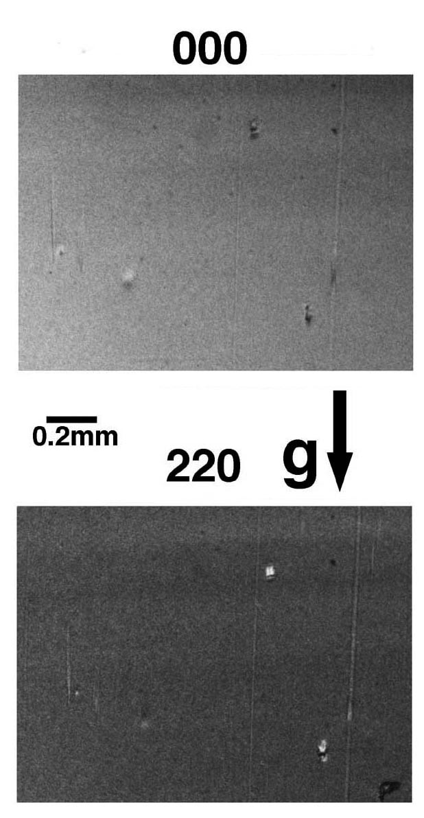
Plane-wave x-ray topography is a high-sensitive technique to visualize imperfection or inhomogeneity in a crystal. Using short wavelength and large beam size plane-wave X-rays, one can perform simple and stable plane-wave x-ray topographic study of lattice defects in a crystal. The figures show the plane-wave X-ray topographs of 000 and 220 reflections of an as-grown CZ-silicon crystal. These topograph images reveal the density and size of the defects, and the magnitude of the lattice strain around the defects.
[ S. Iida, S. Kawado, T. Maehara, Y. Chikaura, Y. Suzuki, K. Kajiwara, J. Matsui, S. Kimura, Journal of Physics D 38, A23-A27 (2005), Fig. 4,
©2005 Institute of Physics and IOP Publishing, Ltd. ]
Source of the figure
Original paper/Journal article
Journal title
S. Iida et al, J. Phys. D: Appl. Phys. 38 (2005) A23-A27.
Figure No.
Technique
Source of the figure
No figure
Required time for experimental setup
3 shift(s)
Instruments
References
| Document name |
|---|
| S. Iida et al, J. Phys. D: Appl. Phys. 38 (2005) A23-A27. |
Related experimental techniques
Questionnaire
The measurement was possible only in SPring-8. Impossible or very difficult in other facilities.
This solution is an application of a main instrument of the beamline.
Ease of measurement
Middle
Ease of analysis
Easy
How many shifts were needed for taking whole data in the figure?
Two-three shifts