New topographic method of detecting microdefects using weak-beam topography with white X-rays
問い合わせ番号
SOL-0000001011
ビームライン
BL28B2(白色X線回折)
学術利用キーワード
| A. 試料 | 無機材料, 計測法、装置に関する研究 |
|---|---|
| B. 試料詳細 | 半導体, 結晶 |
| C. 手法 | X線回折 |
| D. 手法の詳細 | |
| E. 付加的測定条件 | 二次元画像計測 |
| F. エネルギー領域 | X線(4~40 keV) |
| G. 目的・欲しい情報 | 欠陥、転位、歪み |
産業利用キーワード
| 階層1 | 半導体 |
|---|---|
| 階層2 | シリコン系半導体 |
| 階層3 | SOI,基板 |
| 階層4 | 格子定数 |
| 階層5 | イメージング |
分類
A80.12 半導体・電子材料, M10.10 単結晶回折
利用事例本文
X-ray topography is one of powerful methods for the direct observation of lattice defects in nearly perfect crystals. By the weak-beam method, faint kinematical images of microdefects are observed with minimized dynamical background intensity using the interference effects of x-rays in a sample crystal. Figure shows the capability of the method by observing A-swirl defects in floating-zone (FZ) silicon. The dynamical background intensity is markedly reduced, and weak kinematical images could be observed.
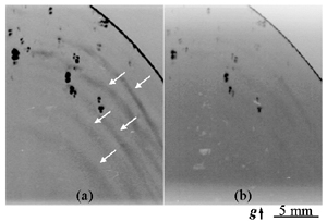
Fig. Topographs of FZ-Silicon (a) without and (b) with dynamical diffraction.
(b) shows a conventional topograph. Arrows indicate the kinematical images.
[ K. Kajiwara, S. Kimura and Y. Chikaura, Japanese Journal of Applied Physics 44, 4211-4212 (2005), Fig. 4,
©2005 The Japan Society of Applied Physics ]
画像ファイルの出典
原著論文/解説記事
誌名
Kentaro Kajiwara, Shigeru Kimura and Yoshinori Chikaura Japanese Journal of Applied Physics Vol.44, No.6A, 2005, pp.4211-4212
図番号
4
測定手法
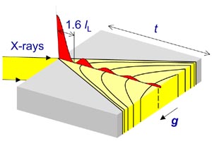
Fig.1 Intensity distribution of Pendellösung fringe arising in Borrmann fan.
The solid lines show the peak of intensity.
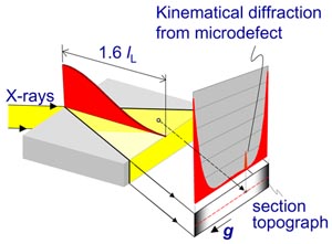
Fig.2 Intensity distribution and section topograph under the condition of T = 1.6lL .
The dynamical diffraction is suppressed except for the marginal region.
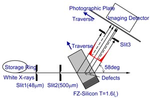
Fig.3 The experimental arrangement of the weak beam topography
with white X-rays in Laue geometry (side view).
画像ファイルの出典
私信等、その他
詳細
XTOP2004ポスターP34
測定準備に必要なおおよその時間
8 時間
測定装置
| 装置名 | 目的 | 性能 |
|---|---|---|
| Imaging Plate | Imaging detecter |
参考文献
関連する手法
アンケート
測定の難易度
中程度
データ解析の難易度
中程度
図に示した全てのデータを取るのにかかったシフト数
2~3シフト