Reciprocal space mapping
Inquiry number
SOL-0000001061
Beamline
BL29XU (RIKEN Coherent X-ray Optics)
Scientific keywords
| A. Sample category | inorganic material |
|---|---|
| B. Sample category (detail) | crystal |
| C. Technique | X-ray diffraction |
| D. Technique (detail) | single crystal |
| E. Particular condition | |
| F. Photon energy | X-ray (4-40 keV) |
| G. Target information | local structure, dislocation, strain |
Industrial keywords
| level 1---Application area | Semiconductor |
|---|---|
| level 2---Target | silicon semiconductor, compound semiconductor |
| level 3---Target (detail) | gate insulator, interlayer insulator, SOI, substrate |
| level 4---Obtainable information | surface,interface, d-spacing (lattice parameter), local structure |
| level 5---Technique | reflectometry, X-ray diffraction |
Classification
A80.12 semiconductor
Body text
Reciprocal space mapping gives the knowledge of intensity distribution in the reciprocal space, which relates, for example, fluctuation of lattice constant and tilt of the lattice plane. Such information is difficult to be extracted from rocking curve measurements and x-ray topography.
The following figures show reciprocal space maps of synthetic diamonds. Sample (a) had stronger oblique streaks than sample (b), which indicated the sample (a) included more 111 stacking faults. No sign of stacking fault was observed for sample (c), however, the horizontal streak indicated bend of the lattice plane.
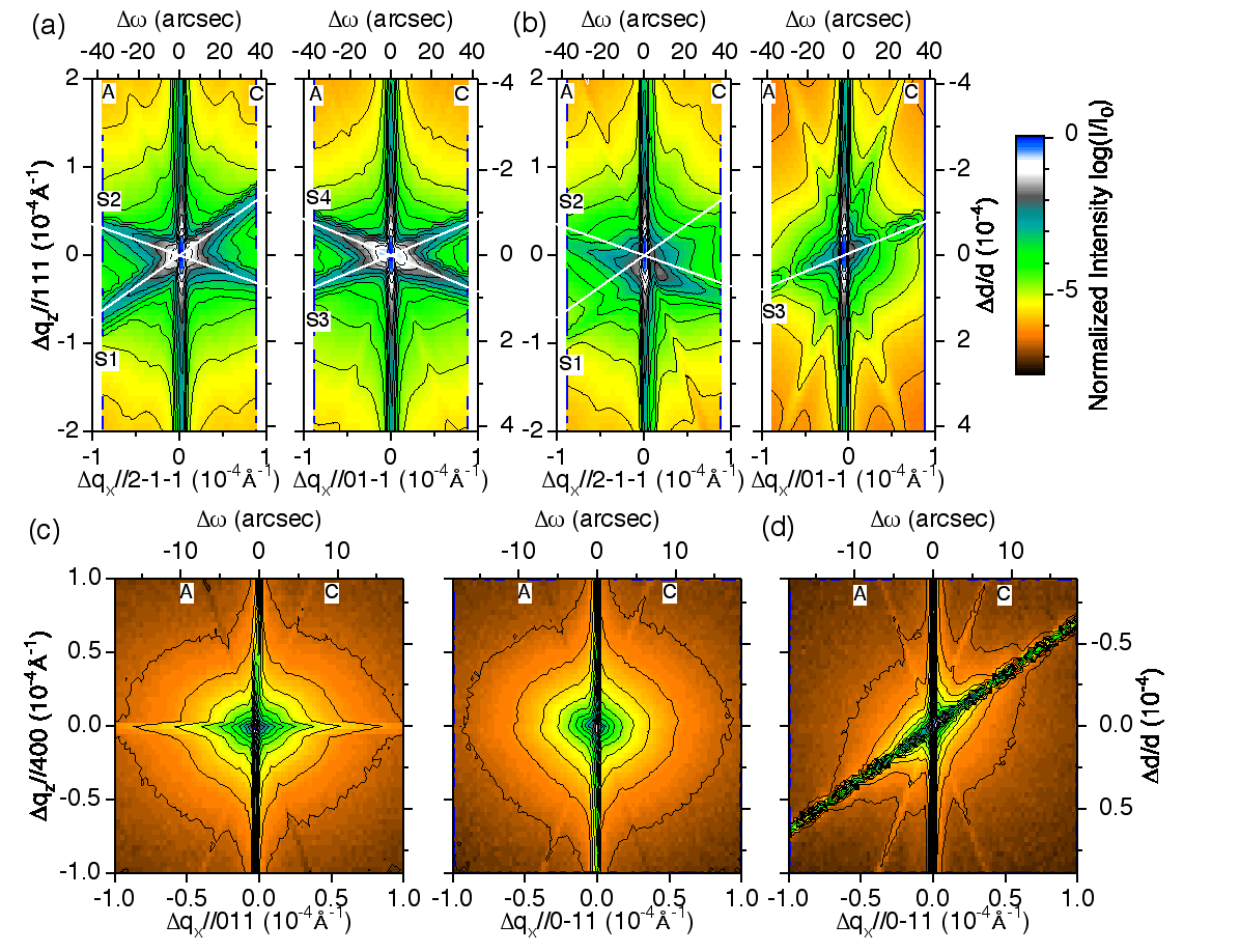
[ K. Tamasaku, T. Ueda, D. Miwa and T. Ishikawa, Journal of Physics D 38, A61-A66 (2005), Fig. 3,
©2005 Institute of Physics and IOP Publishing, Ltd. ]
Source of the figure
Original paper/Journal article
Journal title
K. Tamasaku et al, J. Phys. D: Appl. Phys. 38, A61 (2005)
Figure No.
Technique
Prepare collimator and analyzer crystals which have a lattice constant close to the sample.
Set the collimator, the sample, and the analyzer non-dispersively, and find reflections for all crystals.
Scan the sample and the analyzer so as to map out the region of interest in the reciprocal space.
Source of the figure
No figure
Required time for experimental setup
1 day(s)
Instruments
| Instrument | Purpose | Performance |
|---|---|---|
| goniometers | to align the crystals | 1/720000 deg. angular resolution |
References
| Document name |
|---|
| A.Iida, and K.Kohra, Phys. Status Solidi a 51, 533 (1990). |
| K.Tamasaku, T. Ueda, D. Miwa, and T. Ishikawa, J. Phys. D: Appl. Phys. 38, A61 (2005). |
Related experimental techniques
x-ray topography
rocking curve
Questionnaire
This solution is an application of a main instrument of the beamline.
Ease of measurement
Middle
Ease of analysis
Middle
How many shifts were needed for taking whole data in the figure?
Four-nine shifts