Development of High-Resolution X-ray Microscopy with Wide Field of View Capable of Element Mapping (Press Release)
- Release Date
- 28 Sep, 2011
- BL29XU (RIKEN Coherent X-ray Optics)
Osaka University
Nagoya University
RIKEN
Key research findings
• Visualization of distributions of electron density and specific elements in thick samples that cannot be observed by electron microscopy
• Seamless observation with a spatial resolution from 10 nm to 10 µm
A research group led by Yukio Takahashi (Associate Professor of Graduate School of Engineering, Osaka University), Nobuyuki Zettsu (Associate Professor of Graduate School of Engineering, Nagoya University), and Tetsuya Ishikawa (Chief Scientist and Director of RIKEN SPring-8 Center) has developed an X-ray microscopy technique that enables the observation of the distributions of electron density and specific elements in materials with a wide field of view and a high spatial resolution. For the advancement of nanotechnologies and nanoscience, methods of evaluating the structure and element distribution of materials with various spatial resolutions are essential. Scientists in the group have developed an X-ray microscopy technique that enables seamless observation with a spatial resolution from 10 nm (1 nm = 10-9 m) to 10 µm (1 µm = 10-6 m), or ptychographic X-ray diffraction microscopy for element mapping, using the RIKEN Physics Beamline I (BL29XUL) at SPring-8. They succeeded in visualizing the distribution of electron density for a few hundred different Au/Ag core-shell nanoparticles with a diameter of approximately 200 nm and the distribution of Au atoms at a resolution of approximately 10 nm in a single measurement. Ptychographic microscopy is particularly effective for observing samples whose structure and element distribution must be analyzed at multiple scales to clarify the origin of the expression of functions, such as ultrafine metal particles and brain nerve cells. The resolution and rate of ptychographic imaging can be further improved once next-generation synchrotron radiation, which is now under discussion as a future SPring-8 project, becomes available. Ptychographic imaging will become, for example, capable of visualizing the three-dimensional structure of individual biological cells with a spatial resolution of 10 nm, enabling us to fundamentally understand the life-related functions of organisms. This research was carried out as part of the project "Bulk Nanostructured Metals – A New Structure Material Full of Unexpectedness" (Representative: Nobuhiro Tsuji of Kyoto University), supported by Grants-in-Aid for Scientific Research on Innovative Areas from the Ministry of Education, Culture, Sports, Science and Technology and Japan Society for the Promotion of Science, and also as part of the project "Establishment of Coherent X-ray Diffraction Microscopy for Element Mapping and Analysis of 4D Nano-Meso Structure of Metals" (Representative: Yukio Takahashi) supported by Grants-in-Aid for Young Scientists (A). The research results were published online in the American scientific journal Applied Physics Letters on 28 September 2011. Publication: |
<<Figures>>
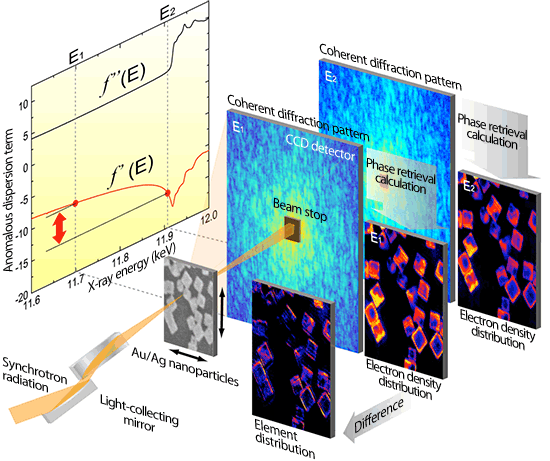
Synchrotron radiation X-rays are focused on a spot with a diameter of a few hundred nanometers through a light-collecting mirror, and a sample (Au/Ag core-shell nanoparticles) is placed along the focal plane. While the sample is two-dimensionally scanned, the intensity distribution of X-rays that are elastically scattered forward at each point (coherent diffraction pattern) is measured with an X-ray charge coupled device (CCD) detector. X-ray energies set to two energy levels below the absorption edge of the element of interest are used to measure the coherent diffraction patterns. A phase retrieval calculation is then performed on the coherent diffraction patterns to obtain the electron density distribution of the sample. Moreover, the distribution map of the target element, whose X-ray energies were used when considering the absorption edge, is extracted by calculating the difference between the electron densities for the two energies.
of Au/Ag core-shell nanoparticles
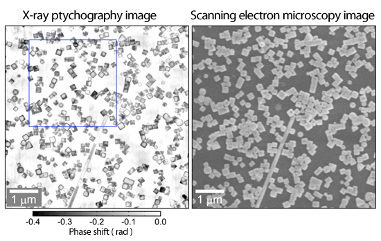
In the ptychographic X-ray diffraction image, the hollow structures of a few hundred Au/Ag core-shell nanoparticles and nanorods are clearly observed, making it possible to quantify the degree of phase shift (electron density distribution). The pixel size in the ptychographic X-ray image is 8.4 nm. In the scanning electron microscopy image, however, only the nanoparticle surfaces are observed and no inner structures are observed.
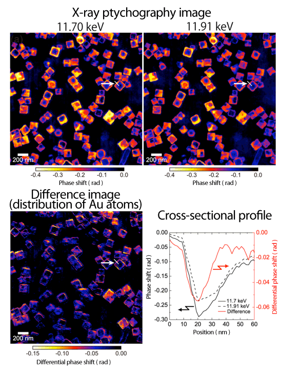
image (used for element mapping) of Au/Ag core-shell
nanoparticles for X-ray energies of 11.70 and 11.91 keV and
cross-sectional profile of single nanoparticle
When the measurement is carried out for two X-ray energies that have very different real parts of the anomalous dispersion term and are lower than the Au L3 edge (11.920 keV), the difference image obtained from the ptychographic images indicates the distribution of Au atoms. Au atoms are locally distributed on the surface of each nanoparticle.
|
For more information, please contact: |

- Previous Article
- Discovery of New Iron-Platinum-Based High-Temperature Superconductor (Press Release)
- Current article
- Development of High-Resolution X-ray Microscopy with Wide Field of View Capable of Element Mapping (Press Release)