Demonstration of Ultrafast Switching in Piezoelectric Thin Film with Nanodomain Structure (Press Release)
- Release Date
- 13 Dec, 2011
- BL13XU (Surface and Interface Structures)
Japan Synchrotron Radiation Research Institute (JASRI)
Tokyo Institute of Technology
National Institute for Materials Science (NIMS)
Kyoto University
Scientists from JASRI, in cooperation with scientists from Tokyo Institute of Technology, NIMS, and Kyoto University, confirmed, for the first time in the world, that ultrafast switching in a time scale as short as 200 ns*1 (two ten-millionths of a second) is possible in a new piezoelectric thin film with microscopic regions called nanodomains. Such piezoelectric thin films are expected to further increase switching speeds. Piezoelectric thin films*2 have been used as power sources for micro-electromechanical systems (MEMS)*3 used in inkjet printers, utilizing their property that structural changes are induced by electrical signals. For current piezoelectric thin films, the switching speed has not been sufficiently reduced, and it is expected that the range of industrial applications of the films will expand and high-performance products will be developed if high-speed switching can be realized. The research group examined the structural changes of nanodomains induced by the application of high-speed pulses of an electric field to a ferroelectric*5 thin film, a type of piezoelectric material, using the high-brilliance synchrotron radiation of SPring-8.*4 The group successfully observed high-speed changes in the orientation of the crystals in the nanodomains, which occur in a time of as short as 200 ns, for the first time in the world. This result demonstrated that switching in piezoelectric thin films can be controlled at the nanosecond time scale (200 ns), which is expected to significantly contribute to the development of high-performance products through the high-speed operation of MEMS using piezoelectric thin films. For example, microprinting using a smaller amount of ink than that used by conventional ink-jet printers can be realized by increasing the processing speed of the MEMS used to control the application of ink. Also, the adoption of materials with a nanodomain structure as ceramic parts to control the fuel efficiency in automobile engines is expected to improve fuel efficiency and reduce the amount of exhaust gas. This study was carried out by the following members: Osami Sakata (Visiting Scientist) of JASRI, who is also Director of the Synchrotron X-ray Station at SPring-8, Research Network and Facility Services Division, NIMS; Hiroshi Funakubo (Associate Professor) and Tomoaki Yamada (Specially Appointed Assistant Professor; also Associate Professor of the Graduate School of Engineering, Nagoya University, and a researcher participating in the proposal-oriented research promotion program (PRESTO) of the Japan Science and Technology Agency (JST)) of the Interdisciplinary Graduate School of Science and Engineering, Tokyo Institute of Technology; and Daisuke Kan (Assistant Professor) of the Institute for Chemical Research, Kyoto University. The results of this study were published online in the scientific journal Applied Physics Letters, which is a high-impact journal in the field of applied physics, on 4 November 2011. It was also chosen as a selected paper in the Virtual Journal of Nanoscale Science & Technology. Publication: |
<<Glossary>>
*1 Nanosecond
A nanosecond is one-billionth of a second.
*2 Piezoelectric thin films
The piezoelectric effect is an effect by which dielectric polarization is induced in crystals, which depends on the magnitude of pressure induced by an external force. The inverse piezoelectric effect is an effect by which crystals are distorted by the application of electric field. Crystals exhibiting these effects are called piezoelectric materials and those in the form of thin films are called piezoelectric thin films.
*3 Micro-electromechanical systems (MEMS)
MEMS are devices in which machine elements, sensors, actuators, and/or electronic circuits are integrated on a single silicon, glass, or organic-material substrate.
*4 SPring-8
SPring-8 is a facility that generates the world’s highest-performance synchrotron radiations. It is located in Harima Science Garden City in Hyogo prefecture and is owned by RIKEN. JASRI is responsible for its operation, management, and support for users. The name SPring-8 is derived from Super Photon ring-8 GeV. Synchrotron radiation is the narrow and extremely powerful light that is obtained when the direction of electrons accelerated to close to the speed of light is bent using electromagnets. Research in a wide range of fields including nanotechnology, biotechnology, and their industrial applications, has been carried out using the synchrotron radiation at SPring-8. A total of over 14,000 researchers from universities, research institutions, and companies from Japan and overseas annually use the high-tech scientific facilities of SPring-8, which support the advanced science and technology in Japan.
*5 Ferroelectrics
Ferroelectrics are a type of piezoelectric material. Among the piezoelectric materials, ferroelectrics are the only crystals that can reverse the direction of spontaneous polarization when an external electric field is applied.
<<Figures>>
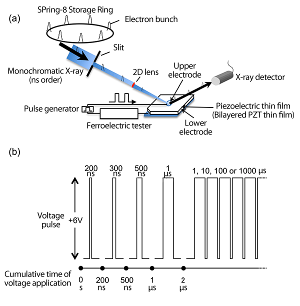
The research group developed and used a measurement system in which high-brilliance X-rays focused to a diameter of several micrometers are irradiated onto an electrode to simultaneously measure the diffracted X-ray intensity and electric polarization while applying a voltage to the electrode with a time resolution of 20-30 ns. In this study, a 200 ns pulse voltage was applied once and then the diffraction profile was recorded. After that, a single pulse with a slightly smaller width was applied and the diffraction profile was recorded again. This process was repeated in the measurement.
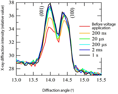
The diffraction peaks from the (001) and (100) planes of the thin-film sample correspond to different crystal orientations in the microdomains of the thin film. Changes in the two diffraction peaks were observed when the pulse width was 200 ns, which demonstrates the high-speed switching of the crystal orientation in microdomains.
|
For more information, please contact: |


- Previous Article
- Establishment of Four-Dimensional (4D) Nano Design, a Technology for the Development of New Materials Used for High-Performance and High-Quality Tires
- Current article
- Demonstration of Ultrafast Switching in Piezoelectric Thin Film with Nanodomain Structure (Press Release)