Fabrication of thin films by pulsed laser deposition

Inquiry number
SOL-0000001057
Beamline
BL23SU (JAEA Actinide Science II)
Scientific keywords
| A. Sample category | inorganic material |
|---|---|
| B. Sample category (detail) | semiconductor, superconductor, magnetic material, ferroelectric material, insulator, ceramics, crystal, membrane |
| C. Technique | absorption and its secondary process, photoemission, photoionization |
| D. Technique (detail) | MCD, LD, photoelectron spectra |
| E. Particular condition | polarization (circular), surface, interface, low-T (~ liquid He), magnetic field (< 2 T), magnetic field (> 2 T) |
| F. Photon energy | soft X-ray, intermediate (2-4 keV) |
| G. Target information | function, electronic state, spin/magnetism |
Industrial keywords
| level 1---Application area | electric component, storage device |
|---|---|
| level 2---Target | condenser, HD,MO |
| level 3---Target (detail) | alignment film, magnetic layer, magnetic head, spin valve |
| level 4---Obtainable information | film thickness, surface,interface, d-spacing (lattice parameter), electronic state, orientation (preferred orientation), magnetic moment, magnetic anisotropy, interface magnetic structure, valence |
| level 5---Technique | XPS, diffraction, XMCD |
Classification
A30.20 surface・interface, A80.14 magnetic materials, A80.30 inorganic material, M40.40 soft x-ray spectroscopy, M50.10 photoelectron spectroscopy
Body text
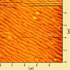
Pulsed laser deposition is a powerful technique for fabrication of thin films such as the transition metal oxide.Figure shows the atomic force microscope image of the SrRuO3 thin film in atmosphere,and it shows clear steps and smooth terrace with atomically flat surface. It indicates that the thin film which fabricated by PLD have suitable surface for the spectrographic measurements such as the Photo electron spectroscopy measurement and the X- ray magnetic circular dichroism.
Source of the figure
Private communication/others
Description
Technique
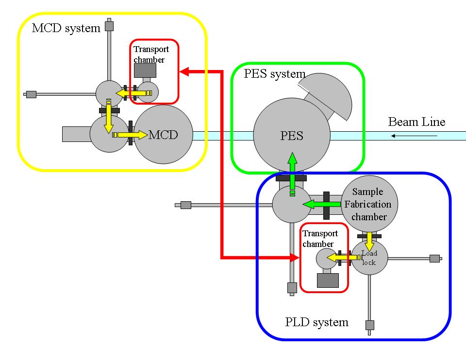
Pulsed laser deposition (PLD) system equips a Nd:YAG laser for ablating sintered targets to prepare thin films. A semiconductor laser used for substrate heating achieves a maximum heating temperature of 1100 degree. Figure shows the schematic image of a sample transfer unit in high vacuum region. PLD system connects directly with a photo electron spectroscopy (PES) system. The thin films prepared by PLD are finally transferred to a soft x-ray magnetic circular dichroism (MCD) system.
Source of the figure
Private communication/others
Description
事例入力者(寺井さん)のデーター
Required time for experimental setup
30 day(s)
Instruments
| Instrument | Purpose | Performance |
|---|---|---|
| Pulsed laser deposition system | Thin film fabrication | Ablation laser : Nd:YAG (266, 355nm), Maximum temperature : 1100deg., 4 multi targets |
| RHEED | estimate of thickness, in-situ surface measurement | |
| Photoemission station | PES, ARPES | direct sample transfer |
| Soft X-ray absorption Magnetic Circular Dichroism apparatus | XAS, MCD | indirect sample transfer |
References
Related experimental techniques
Questionnaire
The measurement was possible only in SPring-8. Impossible or very difficult in other facilities.
This solution is an application of a main instrument of the beamline.
Ease of measurement
With a great skill
Ease of analysis
Middle
How many shifts were needed for taking whole data in the figure?
Less than one shift