Plane-wave x-ray topography

Inquiry number
SOL-0000000986
Beamline
BL29XU (RIKEN Coherent X-ray Optics)
Scientific keywords
| A. Sample category | inorganic material |
|---|---|
| B. Sample category (detail) | crystal |
| C. Technique | X-ray diffraction |
| D. Technique (detail) | |
| E. Particular condition | 2D imaging, room temperature |
| F. Photon energy | X-ray (4-40 keV) |
| G. Target information | dislocation, strain |
Industrial keywords
| level 1---Application area | Semiconductor |
|---|---|
| level 2---Target | silicon semiconductor, compound semiconductor |
| level 3---Target (detail) | SOI, substrate |
| level 4---Obtainable information | d-spacing (lattice parameter), residual stress, structure |
| level 5---Technique | diffraction |
Classification
A80.30 inorganic material, M10.10 single crystal diffraction
Body text
X-ray topography is a method to visualize strain field due to defects in crystals. Such an information makes it possible to judge the quality of crystals, and to determine the way of crystal growth to reduce the defects. The plane-wave topography, which uses plane wave as incidence, is a special technique to investigate minute strain, so that it is useful for nearly perfect crystals. The 1-km beamline at SPring-8 provides wide beam (~30 mm) for large area plane-wave topography, in spite that the source is an undulator.
The following figure is an example of the plane-wave topography measured with a synthetic type IIa diamond. The black parts were the strain fields due to defects, such as stacking faults, outcrops of dislocations, and impurities.
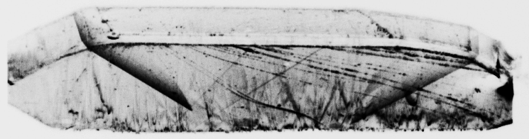
Fig. Plane-wave topograph of a synthetic type IIa diamond.
[ K. Tamasaku, T. Ueda, D. Miwa and T. Ishikawa, Journal of Physics D 38, A61-A66 (2005), Fig. 2(b),
©2005 Institute of Physics and IOP Publishing, Ltd. ]
Source of the figure
Original paper/Journal article
Journal title
K. Tamasaku et al, J. Phys. D: Appl. Phys. 38, A61 (2005)
Figure No.
Fig.2(b)
Technique
Prepare a collimator crystal, which has a similar d-spacing to the reflecting netplane of the sample.
Set the collimator and the sample non-dispersively.
Take pictures by a CCD-based beam monitor.
Source of the figure
No figure
Required time for experimental setup
hour(s)
Instruments
| Instrument | Purpose | Performance |
|---|---|---|
| goniometers | to align the collimator and the samples | 1/720000 deg. angular resolution |
| beam monitor | to take the beam images | 6 or 12 micron pixel size |
References
| Document name |
|---|
| T. Ishikawa, J. Cryst. Growth 103, 131 (1990). |
| K.Tamasaku, T. Ueda, D. Miwa, and T. Ishikawa, J. Phys. D: Appl. Phys. 38, A61 (2005). |
Related experimental techniques
Cathode luminescence
Questionnaire
The measurement was possible only in SPring-8. Impossible or very difficult in other facilities.
This solution is an application of a main instrument of the beamline.
Ease of measurement
Middle
Ease of analysis
Middle
How many shifts were needed for taking whole data in the figure?
Two-three shifts