Clarification of Electronic Structure of Metal Layer Formed at Interface between Two Insulators (Press Release)
- Release Date
- 03 Jun, 2013
- BL23SU (JAEA Actinide Science)
Osaka University
Japan Atomic Energy Agency
Konan University
University of Würzburg (Germany)
Key achievements
• The electronic state of the ultrathin metal layer formed at the interface between two insulators, La and Ti oxides, was directly mapped using soft X-ray synchrotron radiation.
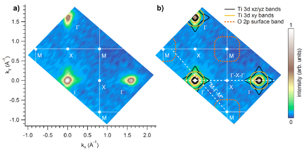
• The energy and momentum of electrons in the metal layer originating from the “buried” interface were simultaneously measured by angle-resolved photoelectron spectroscopy.
|
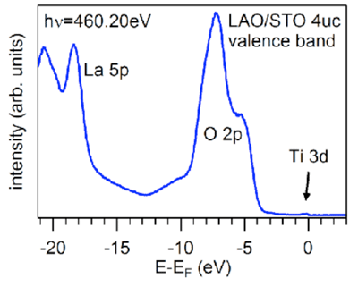
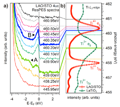
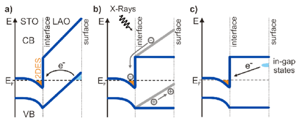
A group led by Shigemasa Suga (specially appointed professor) of the Institute of Scientific and Industrial Research, Osaka University; Akira Sekiyama (professor) and Hidenori Fujiwara (assistant professor) of the Graduate School of Engineering Science, Osaka University; and Atsushi Yamasaki (associate professor) of Konan University carried out joint research in cooperation with Ralph Claessen (professor) and Michael Sing (senior scientist) of the University of Würzburg in Germany and Yuji Saitoh (associate chief scientist) of Japan Atomic Energy Agency. They clarified, for the first time in the world, details of the electronic state that only develops in the ultrathin metal layer formed at the interface between two insulators (La and Ti oxides) using the world’s highest-performance soft X-ray angle-resolved photoelectron spectrometer at the SPring-8 beamline BL23SU owned by Japan Atomic Energy Agency. SrTiO3 (STO) and LaAlO3 (LAO) are ternary oxides and good insulators. When several LAO unit layers are grown on an STO substrate, free electrons are generated at the interface between the two oxides to form a two-dimensional electron system that has high potential for use in practical applications. Such a novel ultrathin metal layer between two thin insulating layers that can be formed with a very small thickness is highly stable against changes in external environmental conditions and is extremely promising for use as a functional nanomaterial. Depending on the growth conditions, a ferromagnetic phase is maintained near the interface, even above 200 K, and diamagnetic/paramagnetic phases also exist below 60 K. Moreover, a two-dimensional superconducting phase appears below a low temperature of 120 mK. Thus, the novel metal layer with diverse properties has recently attracted attention. However, LAO/STO samples fabricated by different research groups around the world have exhibited considerably different physical properties, making the study of these samples difficult. The formation of the metal layer also depends on the thickness of the LAO layers. It has remained unclear whether ferromagnetic and superconducting phases coexist or exist separately in the samples. Clarification of the properties of this novel layer is an urgent task. In this study, the scientists used an LAO/STO sample fabricated by a research group from the University of Augsburg in Germany. This group has long been fabricating the world’s most stable LAO/STO samples with high reproducibility. By performing angle-resolved photoelectron spectroscopy utilizing the world’s highest-performance soft X-rays, the scientists analyzed details of the electronic state of a sample in which an LAO layer with a thickness of four unit cells is grown on an STO substrate to form a stable metal layer at the interface. Resonance photoelectron spectroscopy adopted in this study can be used to detect the Ti 3d electronic state through resonant enhancement using soft X-ray synchrotron radiation with which the excitation of an electron from the Ti 2p shell into the unoccupied Ti 3d conduction band is possible. Fortunately, electrons responsible for superconductivity and ferromagnetism seldom exist in the region outside the interface, which is “buried” under the surface layer, because both STO and LAO have a large band gap. Therefore, only a small number of Ti 3d electrons were successfully detected at the interface by resonance photoelectron spectroscopy with ultrahigh sensitivity. Moreover, the angle-resolved measurement of emitted photoelectrons enabled the evaluation of their momentum. Thus, details of the state of conductive electrons generated at the interface were clarified. In addition to free Ti 3d electrons, localized Ti 3d electrons trapped by O vacancies near the interface in the STO layer also exist. Hence, it was concluded that the localized Ti 3d electrons contribute to the superconductivity and ferromagnetism that have been observed at the interface. This indicates that the widely accepted conventional model is inappropriate. A more feasible model was proposed in which the metal layer is formed at the LAO/STO interface as a result of the transfer of electrons from the O vacancies in the LAO surface to the LAO/STO interface. The achievement of this study is considered revolutionary because it has clarified the electronic state, including the momentum, of the buried interface expected to be used as a functional nanomaterial. The results is published online in the American scientific journal Physical Review Letters on June 14. Publication: |
<<Figures>>
<<Glossary>>
1) Soft X-rays
Although there are several definitions of soft X-rays, here they refer to electromagnetic waves with energies of 200-2000 eV. Soft X-rays have wavelengths in the range of approximately 6-60 Å. Electron (positron) storage rings are the only facilities that can stably generate light with the above ranges of energy and wavelength. The experiments in this study were carried out using soft X-rays at SPring-8.
2) Insulators and metals
Materials that do not allow current to flow are collectively referred to as insulators. Insulators have an energy gap between the filled valence bands and empty conduction bands. Semiconductors have an energy gap smaller than 1 eV and are slightly conductive. Metals have free electrons and no energy gap.
3) Fermi level
Solids have an energy level up to which the bands are filled with electrons and above which the bands are not occupied. This boundary is called the Fermi level. It is important to accurately determine the electronic state near the Fermi level because it primarily determines many physical properties. Clarification of the shape of the Fermi surface in the momentum space is also a key area of research.
4) Resonance photoelectron spectroscopy
When an electron in a filled shell with a deep energy level in an atom constituting a material is excited into an unoccupied conduction band by light such as soft X-rays, a vacancy called a hole is generated in the shell. The energy is stabilized when an electron in the shallow band falls into the hole in the deep band. If this process takes place without photon-emission, another electron in the shallow band is excited into a higher-energy band in accordance with the energy conservation law. The electron in the shallow band can also be directly excited into the higher-energy band by light (this electron is called a photoelectron). Thus the electrons in the shallow band arrive at the same final state through two different paths. As a result of the interference between these two processes, the intensity of the photoelectron emitted from the shallow band greatly increases. This is called resonance photoemission, and spectroscopy using this phenomenon is called resonance photoelectron spectroscopy.
5) Angle-resolved photoelectron spectroscopy
In general, not only energy but also momentum is considered to be conserved among the photoelectron emitted into vacuum and the electrons remaining in a material. However, the momentum of electrons in the direction perpendicular to the surface plane is seldom conserved, requiring further discussion. Measuring the energies of electrons emitted in different directions as a function of angle (equivalent to momentum) can indicate the momentum space where the electrons of the solid existed. This method is called angle-resolved photoelectron spectroscopy.
6) La and Ti
For lanthanum series elements, 1-14 electrons are packed in their 4f orbital. In contrast, for titanium, a 3d transition metal element, two electrons are packed each in the 3d and 4s orbitals before a Ti atom is ionized. Therefore, Ti4+ has no 3d electrons, whereas Ti3+ has a 3d electron (the 3d 1 state). The existence of the 3d electron, or the Ti3+ state, at the LAO/STO interface was proved in this experiment.
|
For more information, please contact: Prof. Akira Sekiyama (OSAKA UNIVERSITY) Assistant Prof. Hidenori Fujiwara (OSAKA UNIVERSITY) Associate Prof. Atushi Yamasaki (KONAN UNIVERSITY) |


- Previous Article
- Direct observation of charge transfer region at interfaces in graphene devices (Press Release)
- Current article
- Clarification of Electronic Structure of Metal Layer Formed at Interface between Two Insulators (Press Release)