Direct observation of charge transfer region at interfaces in graphene devices (Press Release)
- Release Date
- 31 May, 2013
- BL07LSU (University-of-Tokyo Synchrotron Radiation Outstation)
The University of Tokyo
|
Scientists of a research group led by Masaharu Oshima (Professor of the School of Engineering, The University of Tokyo) studied the local electronic states of graphene field effect transistor (FET) devices and succeeded in detecting a charge transfer region at the graphene-channel/metal-electrode interface, which extends over ~500 nm with the energy difference of 60meV. This measurement is achieved by using a scanning photoelectron microscope system enabling three-dimensional nanoscale electron spectroscopy for chemical analysis (3D nano-ESCA) at the University of Tokyo Synchrotron Radiation Outstation Beamline (BL07LSU) at SPring-8. The research group includes Naoka Nagamura (Assistant Professor, Tohoku Universuty), Koji Horiba (Specially Appointed Assistant Professor, KEK), Hirokazu Fukidome (Associate Professor, Tohoku University) and Kosuke Nagashio (Associate Professor, The University of Tokyo); and their colleagues. This result was published in Applied Physics Letters on 17th June, 2013. Publication: |
There has been growing interest in Graphene, which won the Nobel Prize in 2010, because of its exceptional carrier mobility, intriguing electronic properties, possibility for band gap engineering, mechanical superiority, and so on.
Although graphene FETs have been actively studied for post-silicon electronics, the present device characteristics are far restrained from the ideal.
This response deterioration in graphene FETs is considered to be owing to the charge transfer at the graphene/metal-electrode interface.
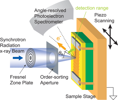
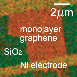
In our study, we have employed nondestructive nanoscale analysis using angle-resolved scanning photoelectron microscopy (3D nano-ESCA, Figure 1) for investigating three dimensional spatial distribution of chemical state at interfaces: graphene/electrode and graphene/substrate. Figure 2 shows an elemental mapping image of the graphene device structure by the photoelectron spectroscopy intensity.
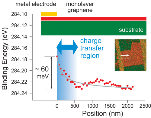
We have demonstrated the charge transfer region at the graphene/electrode interface by detecting the carbon 1s core level shift as a good probe.
The energy shift of 60 meV is clearly detected over the width of 500 nm in the line-profile for the binding energy of graphene (Figure 3).
Furthermore, a depth profiling analysis revealed that the silanol groups at the graphene/substrate interface can affect the charge transfer region at the graphene/electrode interface.
Our experimental technique can clarify the electronic and chemical states of the interfaces which are essential for the device performance.
<<Figures>>
taken along the dashed white line shown in the inset mapping image.
|
For more information, please contact: |

- Previous Article
- World’s First Discovery of Intramolecular Motions of Chaperonin That Plays an Important Role in Protein Repair (Press Release)
- Current article
- Direct observation of charge transfer region at interfaces in graphene devices (Press Release)